L02: The Digital Abstraction
- Encoding Information
- Electricity to the Rescue
- Representing Information with Voltage
- Using Voltages to Encode a Picture
- Information Processing = Computation
- Let’s Build a System!
- Why Did Our System Fail?
- The Digital Abstraction
- Using Voltages Digitally
- Combinational Devices
- A Combinational Digital System
- Is This a Combination Device?
- Dealing With Noise
- Where Does Noise Come From?
- Noise Margins
- Voltage Transfer Characteristic
- VTC Deductions
- VTC Example
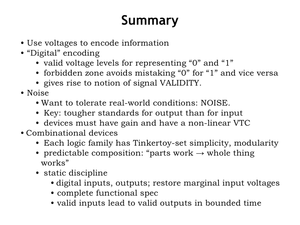
- Summary
Content of the following slides is described in the surrounding text.
In the previous lecture, we discussed how to encode information as sequences of bits. In this lecture, we turn our attention to finding a useful physical representation for bits, our first step in building devices that can process information.
So, what makes a good bit, i.e., what properties do we want our physical representation of bits to have?
Well, we’ll want a lot of them. We expect to carry billions of bits around with us, e.g., music files. And we expect to have access to trillions of additional bits on the web for news, entertainment, social interactions, commerce — the list goes on and on. So we want bits to be small and inexpensive.
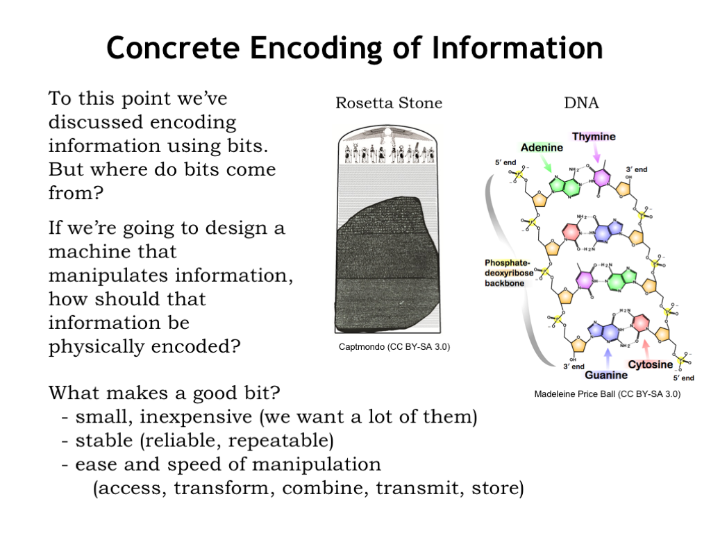
Mother Nature has a suggestion: the chemical encoding embodied in DNA, where sequences of the nucleotides Adenine, Thymine, Guanine and Cytosine form codons that encode genetic information that serve as the blueprint for living organisms. The molecular scale meets our size requirements and there’s active research underway on how to use the chemistry of life to perform interesting computations on a massive scale.
We’d certainly like our bits to be stable over long periods of time — once a 0, always a 0! The Rosetta Stone, shown here as part of its original tablet containing a decree from the Egyptian King Ptolemy V, was created in 196 BC and encoded the information needed for archeologists to start reliably deciphering Egyptian hieroglyphics almost 2000 years later. But, the very property that makes stone engravings a stable representation of information makes it difficult to manipulate the information.
Which brings us to the final item on our shopping list: we’d like our representation of bits to make it easy to quickly access, transform, combine, transmit and store the information they encode.
Assuming we don’t want to carry around buckets of gooey DNA or stone chisels, how should we represent bits?
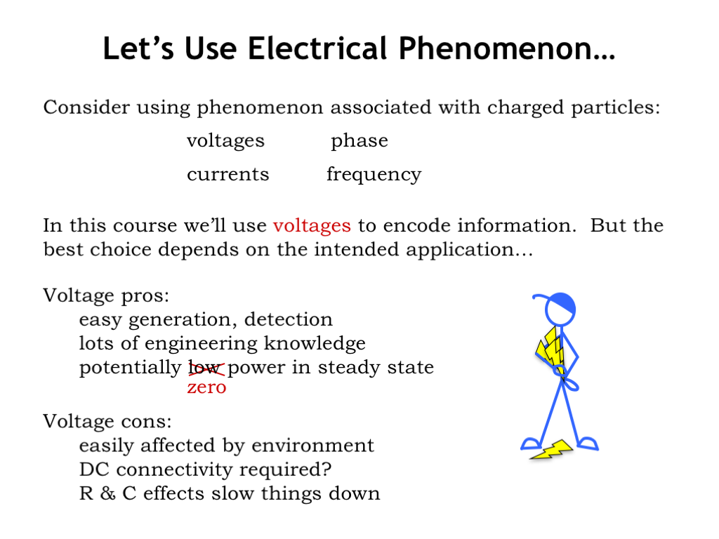
With some engineering we can represent information using the electrical phenomenon associated with charged particles. The presence of charged particles creates differences in electrical potential energy we can measure as voltages, and the flow of charged particles can be measured as currents. We can also encode information using the phase and frequency of electromagnetic fields associated with charged particles — these latter two choices form the basis for wireless communication. Which electrical phenomenon is the best choice depends on the intended application.
In this course, we’ll use voltages to represent bits. For example, we might choose 0V to represent a 0-bit and 1V to represent a 1-bit. To represent sequences of bits we can use multiple voltage measurements, either from many different wires, or as a sequence of voltages over time on a single wire.
A representation using voltages has many advantages: electrical outlets provide an inexpensive and mostly reliable source of electricity and, for mobile applications, we can use batteries to supply what we need. For more than a century, we’ve been accumulating considerable engineering knowledge about voltages and currents. We now know how to build very small circuits to store, detect and manipulate voltages. And we can make those circuits run on a very small amount of electrical power. In fact, we can design circuits that require close to zero power dissipation in a steady state if none of the encoded information is changing.
However, a voltage-based representation does have some challenges: voltages are easily affected by changing electromagnetic fields in the surrounding environment. If I want to transmit voltage-encoded information to you, we need to be connected by a wire. And changing the voltage on a wire takes some time, since the timing of the necessary flow of charged particles is determined by the resistance and capacitance of the wire. In modern integrated circuits, these RC time constants are small, but sadly not zero.
We have good engineering solutions for these challenges, so let’s get started!
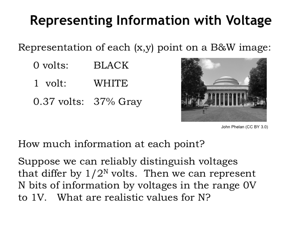
Consider the problem of using voltages to represent the information in a black-and-white image. Each (x,y) point in the image has an associated intensity: black is the weakest intensity, white the strongest. An obvious voltage-based representation would be to encode the intensity as a voltage, say 0V for black, 1V for white, and some intermediate voltage for intensities in-between.
First question: how much information is there at each point in the image? The answer depends on how well we can distinguish intensities or, in our case, voltages. If we can distinguish arbitrarily small differences, then there’s potentially an infinite amount of information in each point of the image. But, as engineers, we suspect there’s a lower-bound on the size of differences we can detect.
To represent the same amount of information that can be represented with N bits, we need to be able to distinguish a total \(2^N\) voltages in the range of 0V to 1V. For example, for N = 2, we’d need to be able to distinguish between four possible voltages. That doesn’t seem too hard — an inexpensive volt-meter would let us easily distinguish between 0V, 1/3V, 2/3V and 1V.
In theory, N can be arbitrarily large. In practice, we know it would be quite challenging to make measurements with, say, a precision of 1-millionth of a volt and probably next to impossible if we wanted a precision of 1-billionth of a volt. Not only would the equipment start to get very expensive and the measurements very time consuming, but we’d discover that phenomenon like thermal noise would confuse what we mean by the instantaneous voltage at a particular time.
So our ability to encode information using voltages will clearly be constrained by our ability to reliably and quickly distinguish the voltage at particular time.
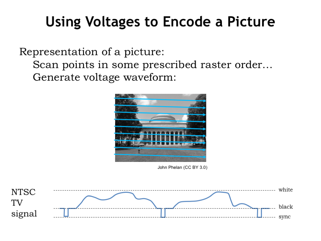
To complete our project of representing a complete image, we’ll scan the image in some prescribed raster order — left-to-right, top-to-bottom — converting intensities to voltages as we go. In this way, we can convert the image into a time-varying sequence of voltages. This is how the original televisions worked: the picture was encoded as a voltage waveform that varied between the representation for black and that for white. Actually the range of voltages was expanded to allow the signal to specify the end of the horizontal scan and the end of an image, the so-called sync signals. We call this a continuous waveform to indicate that it can take on any value in the specified range at a particular point in time.
Now let’s see what happens when we try to build a system to process this signal.
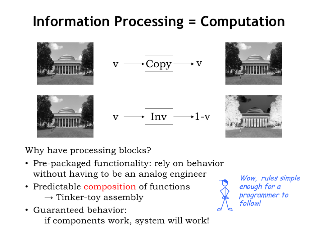
We’ll create a system using two simple processing blocks. The COPY block reproduces on its output whatever voltage appears on its input. The output of a COPY block looks the same as the original image. The INVERTING block produces a voltage of 1-V when the input voltage is V, i.e., white is converted to black and vice-versa. We get the negative of the input image after passing it through an INVERTING block.
Why have processing blocks? Using pre-packaged blocks is a common way of building large circuits — we can assemble a system by connecting the blocks one to another and reason about the behavior of the resulting system without having to understand the internal details of each block. The pre-packaged functionality offered by the blocks makes them easy to use without having be an expert analog engineer!
Moreover, we would we expect to be able to wire up the blocks in different configurations when building different systems and be able to predict the behavior of each system based on the behavior of each block. This would allow us build systems like tinker toys, simply by hooking one block to another. Even a programmer who doesn’t understand the electrical details could expect to build systems that perform some particular processing task.
The whole idea is that there’s a guarantee of predictable behavior: if the components work and we hook them up obeying whatever the rules are for connecting blocks, we would expect the system to work as intended.
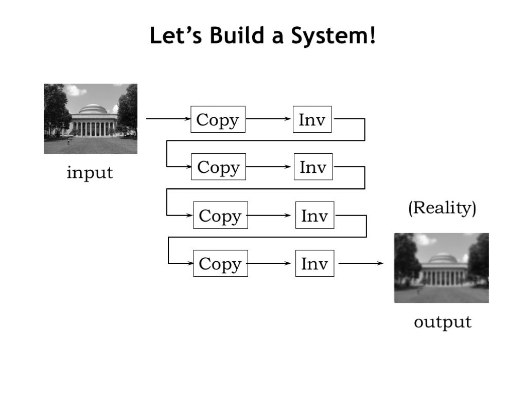
So, let’s build a system with our COPY and INVERTING blocks. Here’s an image processing system using a few instances each block. What do we expect the output image to look like?
Well, the COPY blocks don’t change the image and there are an even number of INVERTING blocks, so, in theory, the output image should be identical to the input image.
But in reality, the output image isn’t a perfect copy of the input, it’s slightly fuzzy — the intensities are slightly off and it looks like sharp changes in intensity have been smoothed out, creating a blurry reproduction of the original. What went wrong?
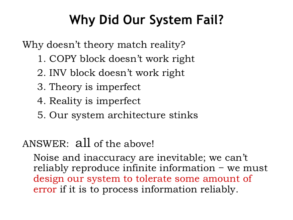
Why doesn’t theory match reality?
Perhaps the COPY and INVERTING blocks don’t work correctly? That’s almost certainly true, in the sense that they don’t precisely obey the mathematical description of their behavior. Small manufacturing variations and differing environmental conditions will cause each instance of the COPY block to produce not V volts for a V-volt input, but V+epsilon volts, where epsilon represents the amount of error introduced during processing. Ditto for the INVERTING block.
The difficulty is that in our continuous-value representation of intensity, V+epsilon is a perfectly correct output value, just not for a V-volt input! In other words, we can’t tell the difference between a slightly corrupted signal and a perfectly valid signal for a slightly different image.
More importantly — and this is the real killer — the errors accumulate as the encoded image passes through the system of COPY and INVERTING blocks. The larger the system, the larger the amount of accumulated processing error. This doesn’t seem so good: it would be awkward, to say the least, if we had to have rules about how many computations could be performed on encoded information before the results became too corrupted to be usable.
You would be correct if you thought this meant that the theory we used to describe the operation of our system was imperfect. We’d need a very complicated theory indeed to capture all the possible ways in which the output signal could differ from its expected value. Those of us who are mathematically minded might complain that “reality is imperfect.” That’s going a bit far though. Reality is what it is and, as engineers, we need to build our systems to operate reliably in the real world. So perhaps the real problem lies in how we chose to engineer the system.
In fact, all of the above are true! Noise and inaccuracy are inevitable. We can’t reliably reproduce infinite information. We must design our system to tolerate some amount of error if it is to process information reliably. Basically, we need to find a way to notice that errors have been introduced by a processing step and restore the correct values before the errors have a chance to accumulate. How to do that is our next topic.
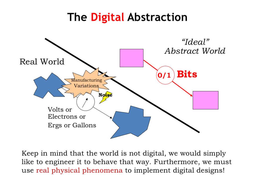
To solve our engineering problem, we will introduce what we’ll call the digital abstraction. The key insight is to use the continuous world of voltages to represent some small, finite set of values, in our case, the two binary values, 0 and 1. Keep in mind that the world is not inherently digital, we would simply like to engineer it to behave that way, using continuous physical phenomenon to implement digital designs.
As a quick aside, let me mention that there are physical phenomenon that are naturally digital, i.e., that are observed to have one of several quantized values, e.g., the spin of an electron. This came as a surprise to classical physicists who thought measurements of physical values were continuous. The development of quantum theory to describe the finite number of degrees of freedom experienced by subatomic particles completely changed the world of classical physics. We’re just now starting to research how to apply quantum physics to computation and there’s interesting progress to report on building quantum computers. But for this course, we’ll focus on how to use classical continuous phenomenon to create digital systems.
The key idea in using voltages digitally is to have a signaling convention that encodes only one bit of information at time, i.e., one of two values, 0 or 1. We’ll use the same uniform representation for every component and wire in our digital system.
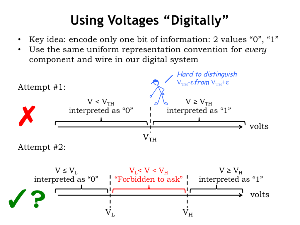
It’ll take us three attempts to arrive at a voltage representation that solves all the problems. Our first cut is the obvious one: simply divide the range of voltages into two sub-ranges, one range to represent 0, the other range to represent 1. Pick some threshold voltage, \(V_{\textrm{th}}\), to divide the range in two. When a voltage V is less than the threshold voltage, we’ll take it to represent a bit value of 0. When a voltage V is greater than or equal to the threshold voltage, it will represent a bit value of 1. This representation assigns a digital value to all possible voltages.
The problematic part of this definition is the difficulty in interpreting voltages near the threshold. Given the numeric value for a particular voltage, it’s easy to apply the rules and come up with the corresponding digital value. But determining the correct numeric value accurately gets more time consuming and expensive as the voltage gets closer and closer to the threshold. The circuits involved would have to be made of precision components and run in precisely-controlled physical environments — hard to accomplish when we consider the multitude of environments and the modest cost expectations for the systems we want to build.
So although this definition has an appealing mathematical simplicity, it’s not workable on practical grounds. This one gets a big red X.
In our second attempt, we’ll introduce two threshold voltages: \(V_{\textrm{L}}\) and \(V_{\textrm{H}}\). Voltages less than or equal to \(V_{\textrm{L}}\) will be interpreted as 0, and voltages greater than or equal to \(V_{\textrm{H}}\) will be interpreted as 1. The range of voltages between \(V_{\textrm{L}}\) and \(V_{\textrm{H}}\) is called the forbidden zone, where we are forbidden to ask for any particular behavior of our digital system. A particular system can interpret a voltage in the forbidden as either a 0 or a 1, and is not even required to be consistent in its interpretation. In fact the system is not required to produce any interpretation at all for voltages in this range.
How does this help? Now we can build a quick-and-dirty voltage-to-bit converter, say by using a high-gain op-amp and reference voltage somewhere in the forbidden zone to decide if a given voltage is above or below the threshold voltage. This reference voltage doesn’t have to be super-accurate, so it could be generated with, say, a voltage divider built from low-cost 10%-accurate resistors. The reference could change slightly as the operating temperature varied or the power supply voltage changed, and so on. We only need to guarantee the correct behavior of our converter for voltages below \(V_{\textrm{L}}\) or above \(V_{\textrm{H}}\).
This representation is pretty promising and we’ll tentatively give it a green checkmark for now. After a bit more discussion, we’ll need to make one more small tweak before we get to where we want to go.
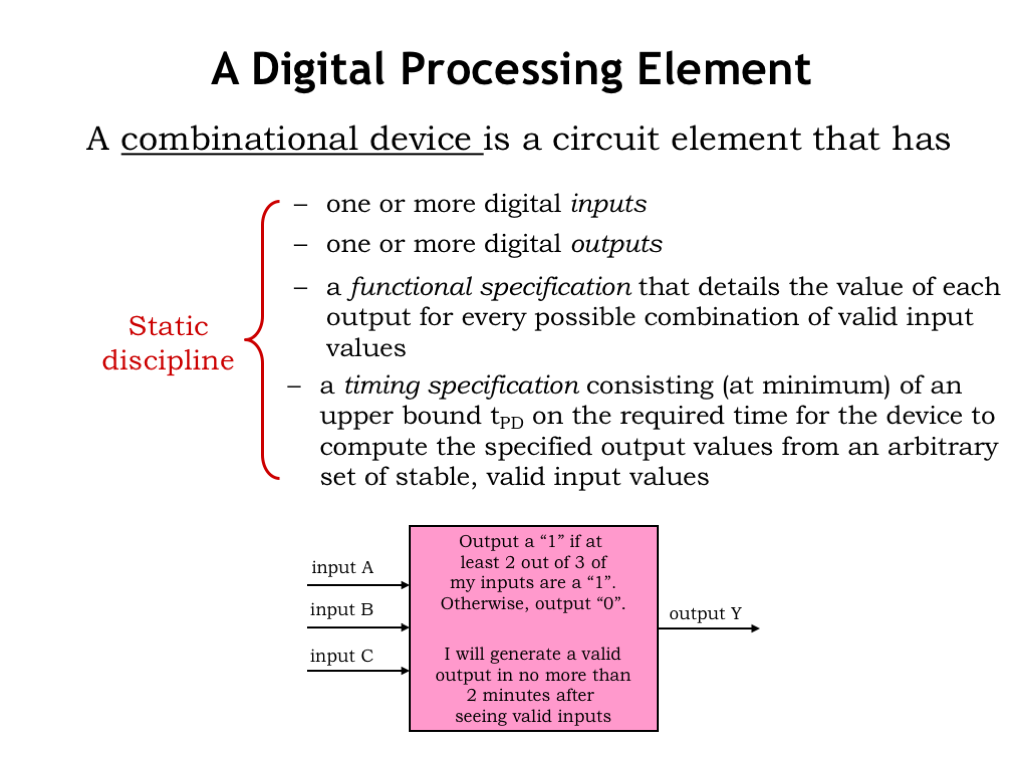
We’re now in a position to define our what it means to be a digital processing element. We say a device is a combinational device if it meets the following four criteria:
First, it should have digital inputs, by which we mean the device uses our signaling convention, interpreting input voltages below \(V_{\textrm{L}}\) as the digital value 0, and voltages above \(V_{\textrm{H}}\) as the digital value 1.
Second, the device’s outputs should also be digital, producing outputs of 0 by generating voltages less than or equal to \(V_{\textrm{L}}\) and outputs of 1 by generating voltages greater than or equal to \(V_{\textrm{H}}\).
With these two criteria, we should be able to hook the output of one combinational device to the input of another and expect the signals passing between them to be interpreted correctly as 0’s and 1’s.
Next, a combinational device is required to have a functional specification that details the value of each output for every possible combination of digital values on the inputs.
In the example, the device has three digital inputs, and since each input can take on one of two digital values, there are 2*2*2 or eight possible input configurations. So the functional specification simply has to tell us the value of the output Y when the inputs are 000, and the output when the inputs are 001, and so on, for all 8 input patterns. A simple table with eight rows would do the trick.
Finally, a combinational device has a timing specification that tells us how long it takes for the output of the dev ice to reflect changes in its input values. At a minimum, there must a specification of the propagation delay, called \(t_{\textrm{PD}}\), that is an upper bound on the time from when the inputs reach stable and valid digital values, to when the output is guaranteed to have a stable and valid output value.
Collectively, we call these four criteria the static discipline, which must be satisfied by all combinational devices.
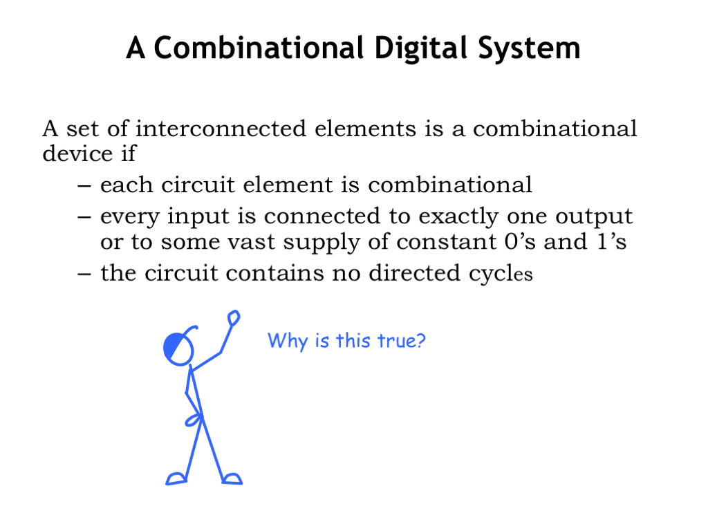
In order to build larger combinational systems from combinational components, we’ll follow the composition rules set forth below.
First, each component of the system must itself be a combinational device.
Second, each input of each component must be connected a system input, or to exactly one output of another device, or to a constant voltage representing the value 0 or the value 1.
Finally, the interconnected components cannot contain any directed cycles, i.e., paths through the system from its inputs to its outputs will only visit a particular component at most once.
Our claim is that systems built using these composition rules will themselves be combinational devices. In other words, we can build big combinational devices out of combinational components. Unlike our flaky analog system from the start of the chapter, the system can be of any size and still be expected to obey the static discipline.
Why is this true?
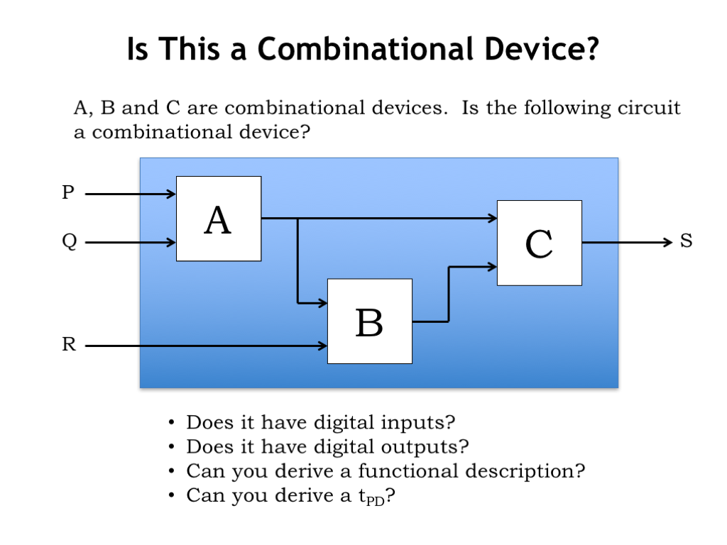
To see why the claim is true, consider the following system built from the combinational devices A, B and C. Let’s see if we can show that the overall system, as indicated by the containing blue box, will itself be combinational. We’ll do this by showing that the overall system does, in fact, obey the static discipline.
First, does the overall system have digital inputs? Yes! The system’s inputs are inputs to some of the component devices. Since the components are combinational, and hence have digital inputs, the overall system has digital inputs. In this case, the system is inheriting its properties from the properties of its components.
Second, does the overall system have digital outputs? Yes, by the same reasoning: all the system’s outputs are connected to one of the components and since the components are combinational, the outputs are digital.
Third, can we derive a functional specification for the overall system, i.e., can we specify the expected output values for each combination of digital input values? Yes, we can by incrementally propagating information about the current input values through the component modules. In the example shown, since A is combinational, we can determine the value on its output given the value on its inputs by using A’s functional specification. Now we know the values on all of B’s inputs and can use its functional specification to determine its output value. Finally, since we’ve now determined the values on all of C’s inputs, we can compute its output value using C’s functional specification. In general, since there are no cycles in the circuit, we can determine the value of every internal signal by evaluating the behavior of the combinational components in an order that’s determined by the circuit topology.
Finally, can we derive the system’s propagation delay, \(t_{\textrm{PD}}\), using the propagation delays of the components? Again, since there are no cycles, we can enumerate the finite-length paths from system inputs to system outputs. Then, we can compute the \(t_{\textrm{PD}}\) along a particular path by summing the \(t_{\textrm{PD}}\)s of the components along the path. The \(t_{\textrm{PD}}\) of the overall system will be the maximum of the path \(t_{\textrm{PD}}\)s considering all the possible paths from inputs to outputs, i.e, the \(t_{\textrm{PD}}\) of the longest such path.
So the overall system does in fact obey the static discipline and so it is indeed a combinational device. Pretty neat — we can use our composition rules to build combinational devices of arbitrary complexity.
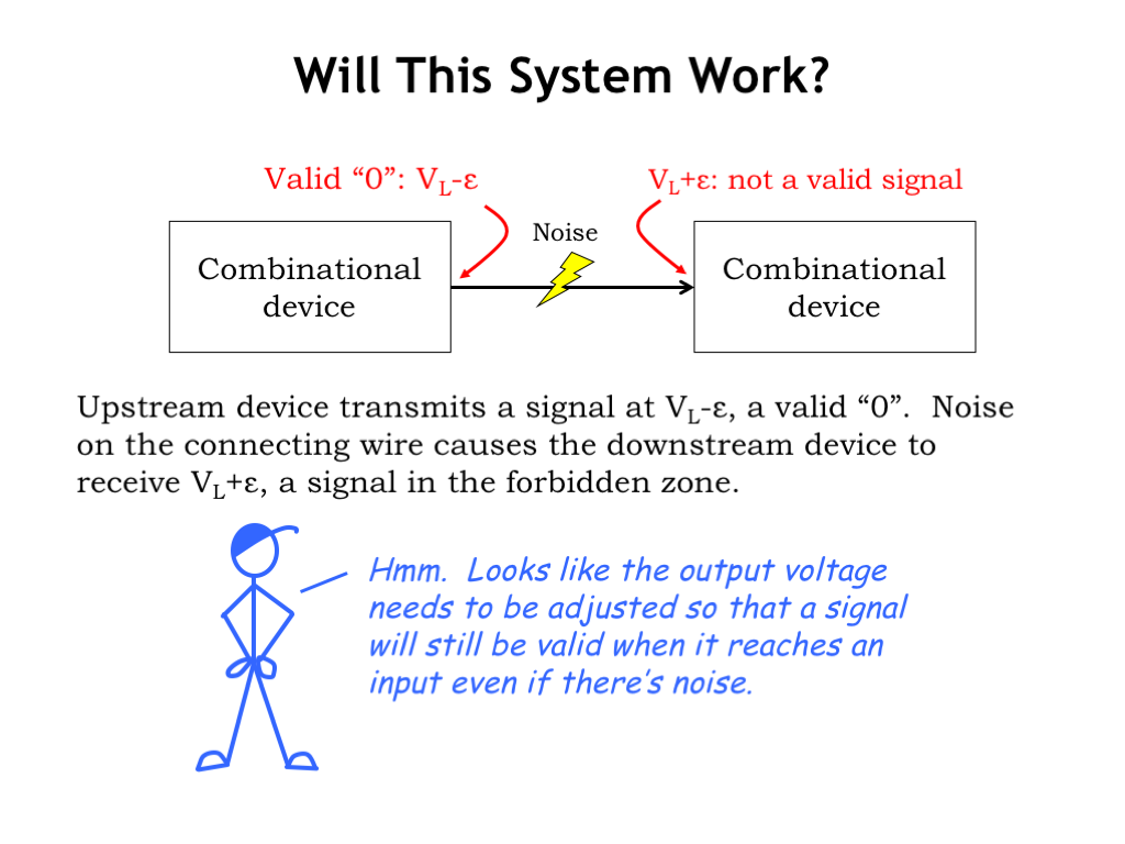
There’s one more issue we need to deal with before finalizing our signaling specification. Consider the following combinational system where the upstream combinational device on the left is trying to send a digital 0 to the downstream combinational device on right. The upstream device is generating an output voltage just slightly below \(V_{\textrm{L}}\), which, according to our proposed signaling specification, qualifies as the representation for a digital 0.
Now suppose some electrical noise slightly changes the voltage on the wire so that the voltage detected on the input of the downstream device is slightly above \(V_{\textrm{L}}\), i.e., the received signal no longer qualifies as a valid digital input and the combinational behavior of the downstream device is no longer guaranteed.
Oops, our system is behaving incorrectly because of some small amount of electrical noise. Just the sort of flaky behavior we are hoping to avoid by adopting a digital systems architecture.
One way to address the problem is to adjust the signaling specification so that outputs have to obey tighter bounds than the inputs, the idea being to ensure that valid output signals can be affected by noise without becoming invalid input signals.
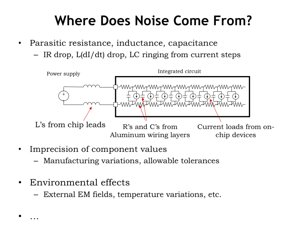
Can we avoid the problem altogether by somehow avoiding noise? A nice thought, but not a goal that we can achieve if we’re planning to use electrical components. Voltage noise, which we’ll define as variations away from nominal voltage values, comes from a variety of sources.
- Noise can be caused by electrical effects such as IR drops in conductors due to Ohm’s law, capacitive coupling between conductors, and L(dI/dt) effects caused by inductance in the component’s leads and changing currents.
- Voltage deviations can be caused manufacturing variations in component parameters from their nominal values that lead to small differences in electrical behavior device-to-device.
- Voltages can be effected by environmental factors such as thermal noise or voltage effects from external electromagnetic fields.
The list goes on! Note that in many cases, noise is caused by normal operation of the circuit or is an inherent property of the materials and processes used to make the circuits, and so is unavoidable. However, we can predict the magnitude of the noise and adjust our signaling specification appropriately — let’s see how this would work.
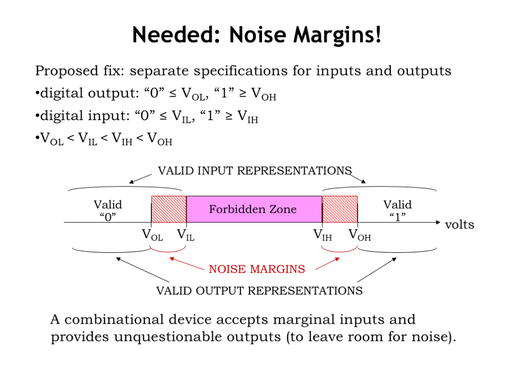
Our proposed fix to the noise problem is to provide separate signaling specifications for digital inputs and digital outputs. To send a 0, digital outputs must produce a voltage less than or equal to \(V_{\textrm{OL}}\) and to send a 1, produce a voltage greater than or equal to \(V_{\textrm{OH}}\). So far this doesn’t seem very different than our previous signaling specification…
The difference is that digital inputs must obey a different signaling specification. Input voltages less than or equal to \(V_{\textrm{IL}}\) must be interpreted as a digital 0 and input voltages greater than or equal to \(V_{\textrm{IH}}\) must be interpreted as a digital 1.
The values of these four signaling thresholds are chosen to satisfy the constraints shown here. Note that \(V_{\textrm{IL}}\) is strictly greater than \(V_{\textrm{OL}}\) and \(V_{\textrm{IH}}\) is strictly less than \(V_{\textrm{OH}}\). The gaps between the input and output voltage thresholds are called the noise margins. The noise margins tell us how much noise can be added to a valid 0 or a valid 1 output signal and still have the result interpreted correctly at the inputs to which it is connected. The smaller of the two noise margins is called the noise immunity of the signaling specification. Our goal as digital engineers is to design our signaling specifications to provide as much noise immunity as possible.
Combinational devices that obey this signaling specification work to remove the noise on their inputs before it has a chance to accumulate and eventually cause signaling errors. The bottom line: digital signaling doesn’t suffer from the problems we saw in our earlier analog signaling example!
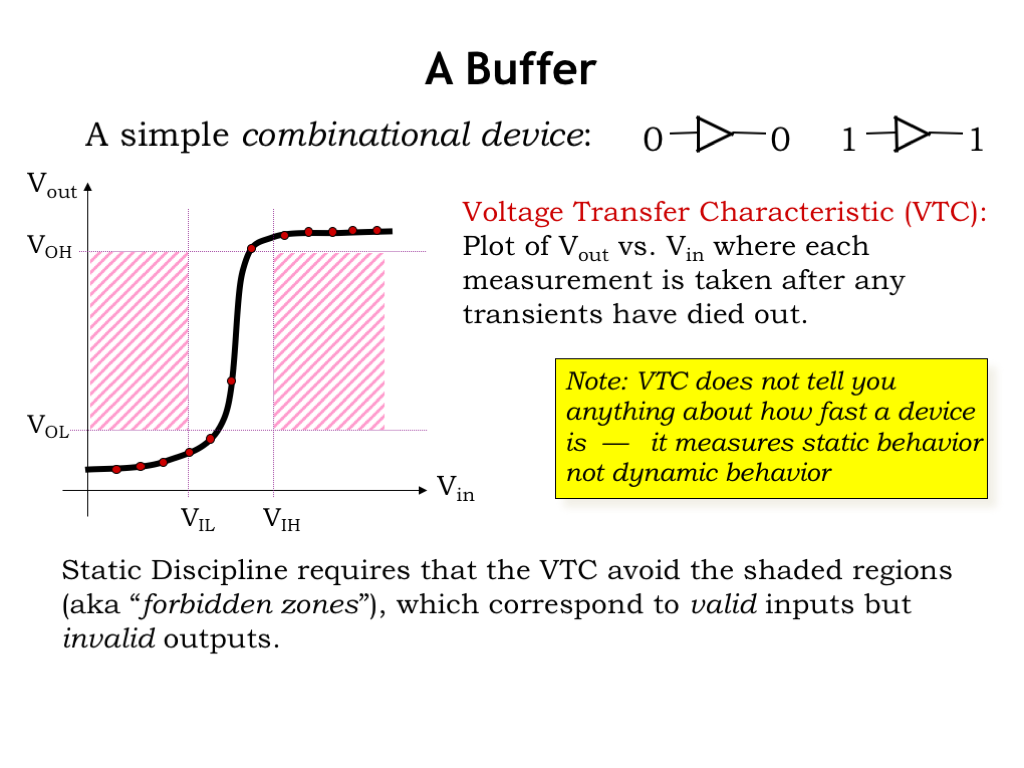
Let’s make some measurements using one of the simplest combinational devices: a buffer. A buffer has a single input and single output, where the output will be driven with the same digital value as the input after some small propagation delay. This buffer obeys the static discipline — that’s what it means to be combinational — and uses our revised signaling specification that includes both low and high noise margins.
The measurements will be made by setting the input voltage to a sequence of values ranging from 0V up to the power supply voltage. After setting the input voltage to a particular value, we’ll wait for the output voltage to become stable, i.e., we’ll wait for the propagation delay of the buffer. We’ll plot the result on a graph with the input voltage on the horizontal axis and the measured output voltage on the vertical axis. The resulting curve is called the voltage transfer characteristic of the buffer. For convenience, we’ve marked our signal thresholds on the two axes.
Before we start plotting points, note that the static discipline constrains what the voltage transfer characteristic must look like for any combinational device. If we wait for the propagation delay of the device, the measured output voltage must be a valid digital value if the input voltage is a valid digital value — “valid in, valid out.” We can show this graphically as shaded forbidden regions on our graph. Points in these regions correspond to valid digital input voltages but invalid digital output voltages. So if we’re measuring a legal combinational device, none of the points in its voltage transfer characteristic will fall within these regions.
Okay, back to our buffer: setting the input voltage to a value less than the low input threshold \(V_{\textrm{IL}}\), produces an output voltage less than \(V_{\textrm{OL}}\), as expected — a digital 0 input yields a digital 0 output. Trying a slightly higher but still valid 0 input gives a similar result. Note that these measurements don’t tell us anything about the speed of the buffer, they are just measuring the static behavior of the device, not its dynamic behavior.
If we proceed to make all the additional measurements, we get the voltage transfer characteristic of the buffer, shown as the black curve on the graph. Notice that the curve does not pass through the shaded regions, meeting the expectations we set out above for the behavior of a legal combinational device.
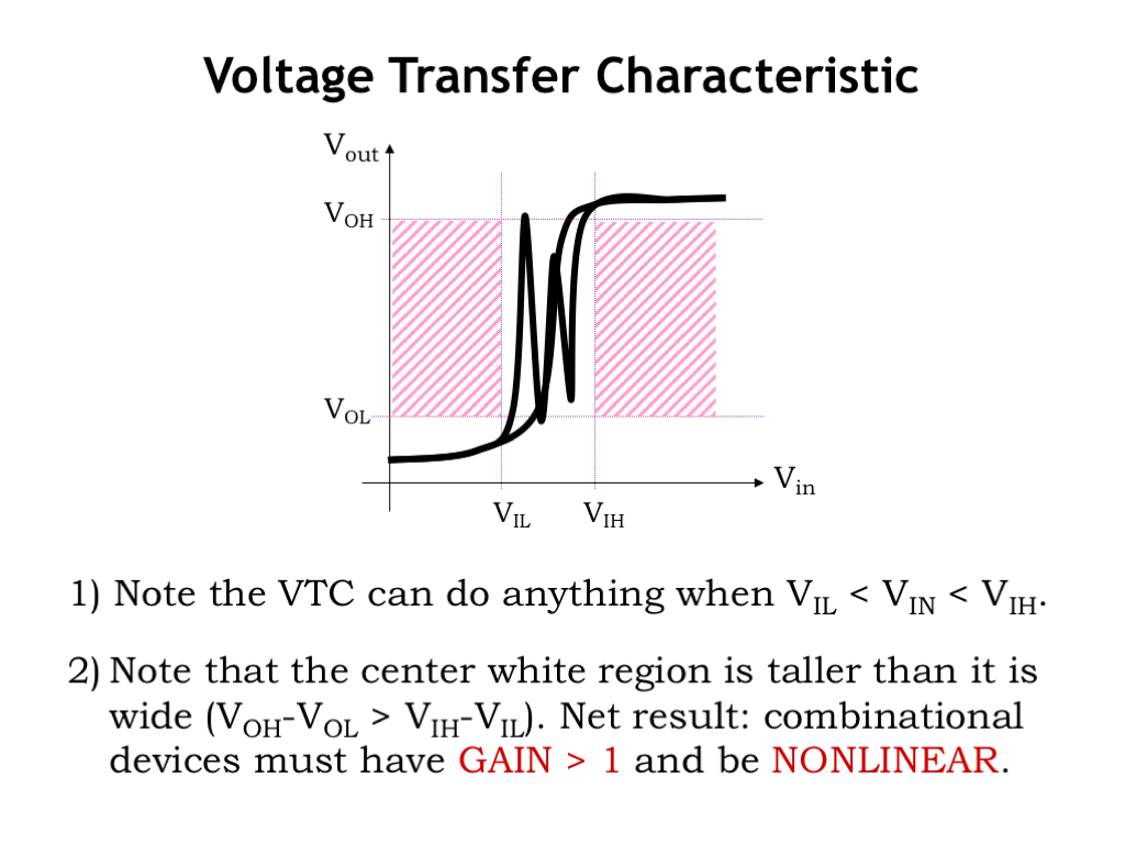
There are two interesting observations to be made about voltage transfer characteristics.
Let’s look more carefully at the white region in the center of the graph, corresponding to input voltages in the range \(V_{\textrm{IL}}\) to \(V_{\textrm{IH}}\). First note that these input voltages are in the forbidden zone of our signaling specification and so a combinational device can produce any output voltage it likes and still obey the static discipline, which only constrains the device’s behavior for *valid* inputs.
Second, note that the center white region bounded by the four voltage thresholds is taller than it is wide. This is true because our signaling specification has positive noise margins, so \(V_{\textrm{OH}}\) – \(V_{\textrm{OL}}\) is strictly greater than \(V_{\textrm{IH}}\) – \(V_{\textrm{IL}}\). Any curve passing through this region — as the VTC must — has to have some portion where the magnitude of the slope of the curve is greater than 1. At the point where the magnitude of the slope of the VTC is greater than one, note that a small change in the input voltage produces a larger change in the output voltage. That’s what it means when the magnitude of the slope is greater than 1. In electrical terms, we would say the device as a gain greater than 1 or less than -1, where we define gain as the change in output voltage for a given change in input voltage.
If we’re considering building larger circuits out of our combinational components, any output can potentially be wired to some other input. This means the range on the horizontal axis (\(V_{\textrm{IN}}\)) has to be the same as the range on the vertical axis (\(V_{\textrm{OUT}}\)), i.e., the graph of VTC must be square and the VTC curve fits inside the square. In order to fit within the square bounds, the VTC must change slope at some point since we know from above there must be regions where the magnitude of the slope is greater than 1 and it can’t be greater than 1 across the whole input range. Devices that exhibit a change in gain across their operating range are called nonlinear devices.
Together these observations tell us that we cannot use only linear devices such as resistors, capacitors and inductors, to build combinational devices. We’ll need nonlinear devices with gain > 1. Finding such devices is the subject of the next chapter.
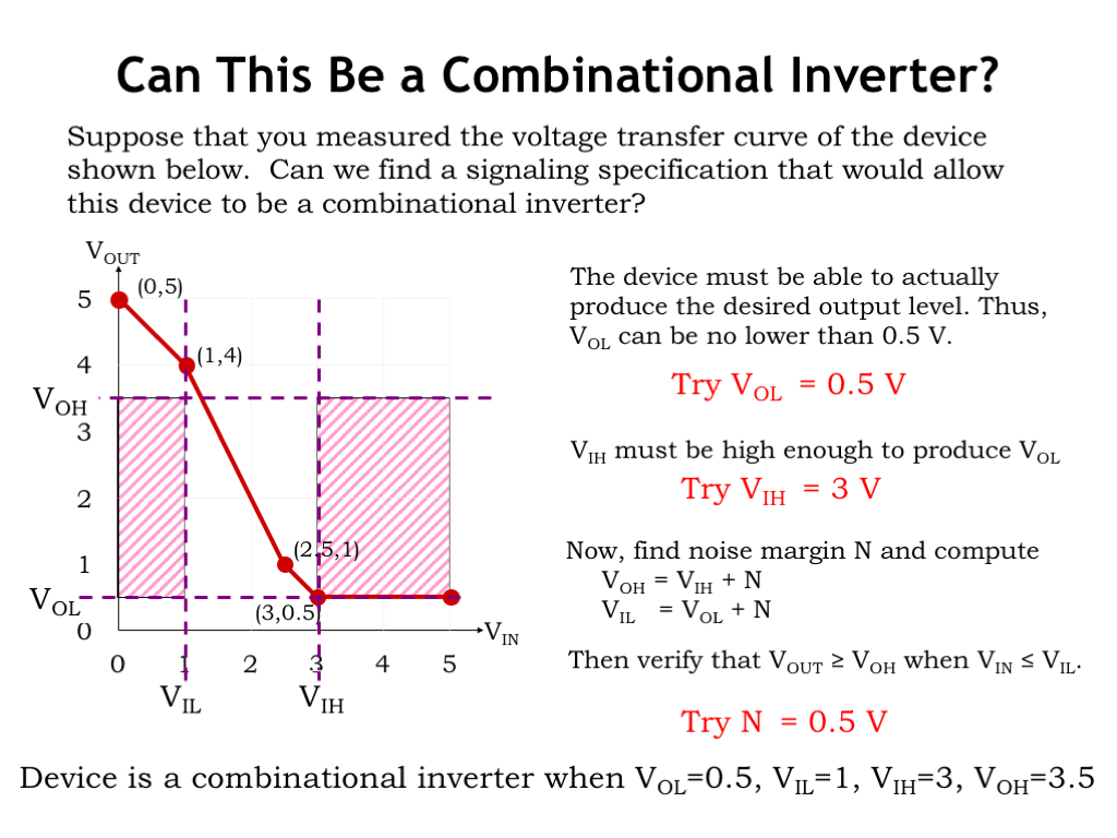
Let’s look at a concrete example. This graph shows the voltage transfer characteristic for a particular device and we’re wondering if we can use this device as a combinational inverter. In other words, can we pick values for the voltage thresholds \(V_{\textrm{OL}}\), \(V_{\textrm{IL}}\), \(V_{\textrm{IH}}\) and \(V_{\textrm{OH}}\) so that the shown VTC meets the constraints imposed on a combinational device?
An inverter outputs a digital 1 when its input is a digital 0 and vice versa. In fact this device does produce a high output voltage when its input voltage is low, so there’s a chance that this will work out.
The lowest output voltage produced by the device is 0.5V, so if the device is to produce a legal digital output of 0, we have to choose \(V_{\textrm{OL}}\) to be at least 0.5V.
We want the inverter to produce a valid digital 0 whenever its input is valid digital 1. Looking at the VTC, we see that if the input is higher than 3V, the output will be less than or equal to \(V_{\textrm{OL}}\), so let’s set \(V_{\textrm{IH}}\) to 3V. We could set it to a higher value than 3V, but we’ll make it as low as possible to leave room for a generous high noise margin.
That takes care of two of the four signal thresholds, \(V_{\textrm{OL}}\) and \(V_{\textrm{IH}}\). The other two thresholds are related to these two by the noise margin N as shown by these two equations. Can we find a value for N such that \(V_{OUT} \ge V_{OH}\) when \(V_{IN} \le V_{IL}\)? If we chose N = 0.5V, then the formulas tell us that \(V_{\textrm{IL}}\) = 1V and \(V_{\textrm{OH}}\) = 3.5V. Plotting these thresholds on the graph and adding the forbidden regions, we see that happily the VTC is, in fact, legal!
So we can use this device as a combinational inverter if we use the signaling specification with \(V_{\textrm{OL}}\) = 0.5V, \(V_{\textrm{IL}}\) = 1V, \(V_{\textrm{IH}}\) = 3V and \(V_{\textrm{OH}}\) = 3.5V. We’re good to go!